

Samsung Electronics has high expectations for the memory chip market in the coming years. According to Song Jai-hyuk, Samsung’s Chief Technology Officer (CTO) for Device Solutions, demand for memory chips, especially from companies building large-scale cloud infrastructures for artificial intelligence (AI) applications, will continue to rise through 2026 and beyond. The growing reliance on AI hyperscalers — companies developing massive cloud systems to support AI needs — has driven unprecedented levels of memory chip orders, significantly boosting prices in the process.
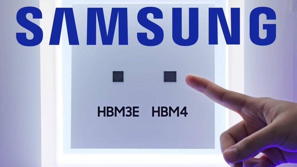
Samsung, a leader in semiconductor manufacturing, is focusing on mass-producing HBM4 (High Bandwidth Memory) chips, which will help meet the expanding demand. Last year, Samsung reported strong sales growth, particularly due to the success of its HBM3E memory format, a trend that continued into the fourth quarter. The new HBM4 chips are expected to drive continued growth in 2026, with feedback from early adopters already praising the performance.
In addition to launching the HBM4 memory, Samsung is also exploring cutting-edge technologies like hybrid bonding and zHBM to improve memory efficiency and bandwidth. The company is also delving into processing-in-memory (PIM) designs, which allow memory chips to perform computations, further enhancing their performance. Samsung’s focus on these innovations positions them to stay at the forefront of the memory chip industry and meet the growing needs of AI hyperscalers.
New Samsung Memory Designs and Technologies
1. HBM4 Memory for Enhanced Performance
The HBM4 memory chips are at the heart of Samsung’s strategy for maintaining high demand in the memory chip market. Early feedback from corporate customers who received shipments of HBM4 has been overwhelmingly positive, with reports of “very satisfactory” performance. HBM4 promises to provide greater bandwidth and efficiency, addressing the increasingly demanding needs of AI applications and cloud infrastructure.
- Mass production of HBM4 began in early 2026, with the first shipments already received by some customers. These chips are expected to handle large-scale data processing with greater speed and reliability than their predecessors.
2. Hybrid Bonding Technology: Reducing Thermal Resistance
In its efforts to improve HBM memory efficiency, Samsung has introduced hybrid bonding technology. This technology helps reduce thermal resistance in 12H and 16H stacks by 20%, resulting in lower temperatures on the base die, with tests showing an 11% reduction in temperature. This innovation is crucial for enhancing the performance and durability of memory chips, especially in high-demand environments like AI data centers.
While Samsung has not yet provided a timeline for when hybrid-bonded dies will be available to consumers, this advancement promises to improve the overall longevity and performance of HBM memory.
3. zHBM: Increasing Memory Bandwidth and Efficiency
Another breakthrough technology Samsung is exploring is zHBM (stacked memory in the Z-axis), which has the potential to increase memory bandwidth by 4x. Additionally, zHBM aims to reduce power consumption by 25%, making it a more efficient solution for high-performance computing tasks. By stacking memory chips in the Z-axis, Samsung can optimize space and performance, making this an exciting development for the future of AI hyperscalers.
4. HBM-PIM: Memory with Compute Capabilities
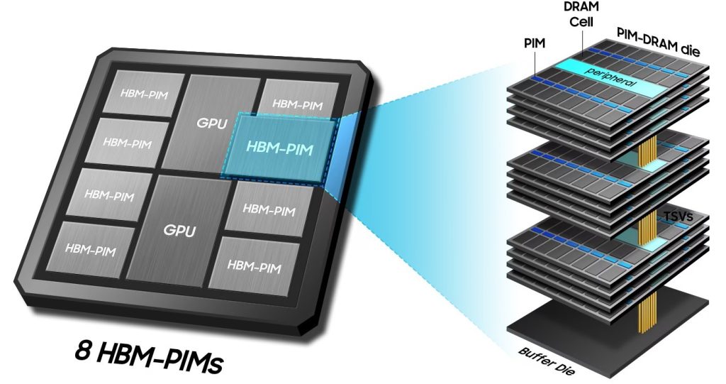
Samsung is also working on a more advanced memory design known as HBM-PIM (processing-in-memory), which integrates compute capabilities directly into memory chips. This design is set to boost performance by a staggering 2.8x while maintaining the same level of power efficiency. The inclusion of compute power within the memory chips could significantly change the way data is processed, enabling faster and more efficient computing for AI tasks.
In collaboration with AMD, Samsung has already tested HBM-PIM memory in a custom AMD Instinct MI100 setup, showing promising results for future implementations.
Samsung’s Vision for the Future
Samsung’s push for next-generation memory technologies, such as HBM4, hybrid bonding, zHBM, and HBM-PIM, is designed to keep pace with the growing demands of AI hyperscalers and other high-performance computing applications. As AI technologies continue to evolve, so too will the need for faster and more efficient memory solutions. Samsung is positioning itself at the forefront of this transformation by developing cutting-edge memory technologies that promise to shape the future of cloud infrastructure and AI applications.
Conclusion: A Bright Future for Samsung’s Memory Chips
With the increasing demand for memory chips driven by AI hyperscalers, Samsung is in a prime position to capitalize on the growth of the industry through its innovative HBM4, hybrid bonding, zHBM, and HBM-PIM technologies. These advancements will help Samsung meet the needs of cloud infrastructure providers, AI researchers, and other data-intensive industries. As the demand for high-performance memory continues to rise, Samsung’s new memory designs will ensure that the company remains at the top of the semiconductor market.